


- Thick Copper PCB (105-240µm)
- Ultra Thick Copper PCB (300-500µm)
- Ultra Max Thick Copper PCB (1000µm)
- Combination PCB
- Bus Bar Embedded PCB
- Copper Inlay PCB
- Aluminum Base PCB


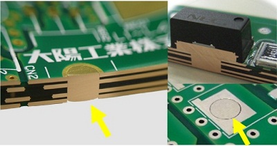
Copper Inlay PCB
With increased use of high performance parts on PCB, heat generation increases and counter-measure for heat dissipation become more important in order to maintain product performance and its life.
Also, miniaturization of parts makes it difficult to get natural heat dissipation from parts themselves.
We need to design PCB to create heat escape through PCB circuit path.
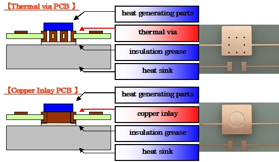
Conventional PCB can't solve such heat problem.PCB with thermal via also has limitation to solve the heat problem.
We offer "Copper Inlay PCB" which can get efficient heat dissipation by pressing copper into the board right under heat generating components.
Strong point of Copper Inlay PCB
- It is possible to exhaust heat efficiently by pressing in copper right under the heat generating components.
- Implementation of cost effective solution for heat dissipation.
- Reliability of solder connecting part will improve because linear expansion coefficient of copper is lower than that of Aluminum of aluminum heat sink.
- More flexible design is possible because we can use high multi layer and both sided board PCB compared with Aluminum based board or heat sink.
Specifications
Inlay Diameter :3φ/5φ/6φ/8φ
Inlay Thickness :0.8-3.2mm
*Board thickness will be more than 1.2mm if inlay diameter is over 6φ.
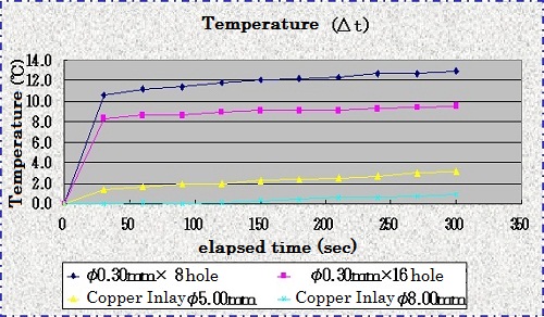
Compared Thermal via PCB with Copper Inlay PCB
Examples of application
- Human android
- Electric Motorcycle
- Forklift
- LED lamp
- Car Electronics
- High Efficiency Server Power Supply
- Inverter
- Others
Auto copper inlay press machine
We can enable mass production by developing auto machine.
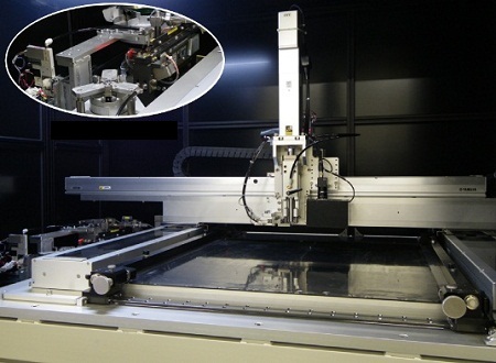
Prepare a line of copper chips, and press head picks up and moves copper chips, and press in chips into designated holes.
- | Top Page |
- Company Profile |
- Contact |
- Privacy Policy |
- | High Current |
- Heat Dissipation |
- Design Team |
- Locations |
| All rights reserved, Copyright 2007(c)TAIYO KOGYO.CO.,LTD. |